 跳到内容
跳到内容 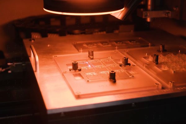
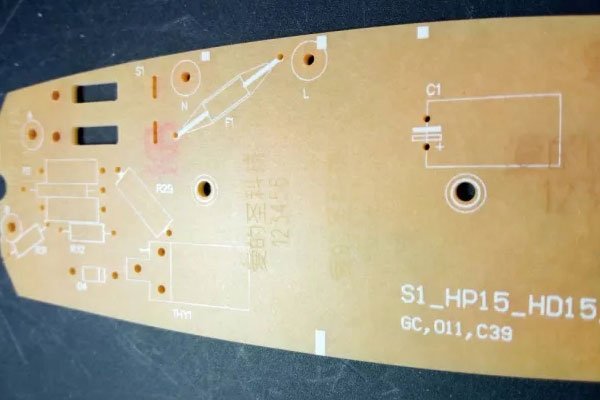
Marking PCBs is a critical step in electronics manufacturing. It ensures traceability1, regulatory compliance, and product identification while preserving the integrity of sensitive components. Achieving precision and efficiency requires the right tools—and in this arena, laser marking technology2 is unmatched.
Among laser options, UV laser marking stands out as the best solution for PCB applications. Its precision, versatility, and minimal thermal impact make it indispensable for modern manufacturing.
At Koolaser, we provide state-of-the-art UV laser marking machines3 tailored for PCB manufacturers, ensuring quality and efficiency in every operation.
PCB marking technologies need to cater to intricate designs and diverse materials while ensuring durability and clarity. The three main types of laser technologies used for PCB marking are CO₂ lasers4, fiber lasers5, and UV lasers6. Each has its unique features and applications.
CO₂, fiber, and UV lasers offer distinct advantages and are selected based on specific PCB marking requirements.
Dive Deeper: Comparison of Laser Technologies for PCB Marking
| Laser Type | Wavelength | Best Materials | Advantages | Disadvantages |
|---|---|---|---|---|
| CO₂ Laser | ~10,600 nm | Organics, glass, some plastics | - Cost-effective for non-metals. - High efficiency for organic substrates. | - Less effective on metals. - Can cause thermal stress on heat-sensitive PCBs. |
| Fiber Laser | ~1,064 nm | Metals (e.g., stainless steel, aluminum) | - High speed and precision for metals. - Durable and long-lasting marks. | - Not suitable for heat-sensitive PCBs. - Potential for thermal damage. |
| UV Laser | ~355 nm | PCBs, ceramics, plastics, thin metals | - Minimal thermal impact. - High precision for intricate designs. | - Higher initial cost compared to CO₂ lasers. |
UV laser marking is widely recognized as the best technology for PCB applications. Its short wavelength (355 nm) allows it to focus tightly, making it ideal for marking intricate details. Unlike CO₂ or fiber lasers7, UV lasers minimize heat transfer to the material, reducing the risk of damage to sensitive components.
UV laser marking achieves superior precision while preserving the integrity of heat-sensitive materials.
Dive Deeper: Key Advantages of UV Laser Marking
-
High Precision:
UV lasers produce extremely fine markings, making them suitable for micro-scale designs, QR codes, and high-density interconnect (HDI) PCBs. -
Minimal Heat Effect:
The cold marking process8 ensures that even delicate substrates like FR4, polyimide, and ceramics remain undamaged. -
Material Versatility:
UV lasers can handle a wide range of materials, from thin metals to organic layers, providing flexibility for diverse PCB designs. -
Environmental Benefits:
Unlike ink-based marking systems9, UV lasers don’t require consumables, reducing waste and operational costs.
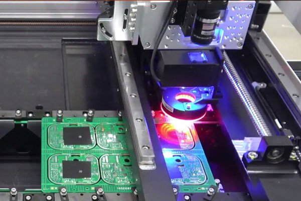
Why Koolaser UV Laser Marking Machines Are Perfect for PCB Applications?
Koolaser’s UV laser marking machines are specifically engineered to meet the high demands of PCB manufacturers. With precision technology, user-friendly features, and robust performance, our machines deliver results that exceed expectations.
Koolaser’s UV laser machines combine innovation and practicality to set a new standard for PCB marking.
Dive Deeper: Features of Koolaser UV Laser Marking Machines
-
Ultra-High Precision:
Koolaser UV lasers excel in achieving micrometer-level accuracy, ideal for compact and intricate PCB layouts. This makes them indispensable for applications like fine-pitch components and multi-layer boards10. -
Minimal Thermal Stress:
By operating at a short wavelength, Koolaser’s UV lasers drastically reduce the heat-affected zone, ensuring no damage to fragile materials or nearby components11. -
Compact Design:
With a lightweight and space-saving form factor, Koolaser machines integrate seamlessly into any production setup, from small workshops to large-scale factories. -
Customizable Settings:
Our machines allow users to adjust speed, frequency, and power to match specific material properties12, ensuring optimal performance across various applications. -
Advanced Cooling System:
Equipped with efficient cooling technology13, Koolaser UV lasers maintain stable operation during continuous high-volume production cycles.
Benefits of Koolaser UV Laser Marking for PCB Manufacturers
Investing in Koolaser UV laser marking machines offers manufacturers numerous benefits, from operational efficiency to product quality.
Koolaser’s UV lasers are designed to enhance productivity while maintaining impeccable marking standards.
Dive Deeper: Why Choose Koolaser for PCB Marking?
| Feature | Koolaser UV Laser Advantage | Manufacturer Benefit |
|---|---|---|
| Speed and Efficiency | High-speed marking capabilities. | Reduces production time and increases throughput, ensuring faster delivery cycles. |
| Durable Markings | Permanent, wear-resistant results | Ensures long-term traceability and compliance with industry standards. |
| Eco-Friendly Technology | No consumables like ink or chemicals. | Minimizes environmental impact and lowers operational costs. |
| Comprehensive Support | Installation, training, and after-sales service | Facilitates seamless integration and ensures reliable, long-term operation. |
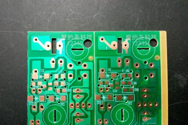
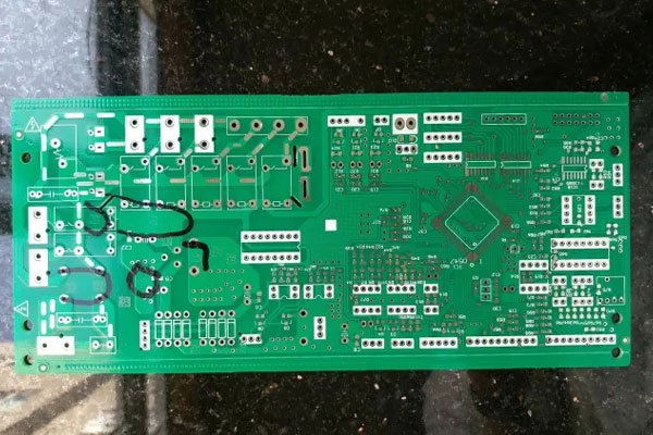
Real-World Applications of Koolaser UV Laser Technology
Koolaser’s UV laser marking machines are trusted by manufacturers across industries, including:
- Electronics Manufacturing: For marking intricate PCBs used in smartphones, laptops, and IoT devices.
- Medical Devices: Ensuring clean and precise markings on sensitive equipment.
- Aerospace and Automotive: High-durability markings for PCB components exposed to extreme conditions.
- Custom Products: Tailoring designs for small-scale manufacturing or prototype development.
Dive Deeper: A Closer Look at PCB Applications
| Application | Koolaser UV Laser Solution | Outcome |
|---|---|---|
| Traceability Codes | Creates QR codes, serial numbers, and barcodes with flawless precision. | Ensures easy tracking and compliance with industry regulations. |
| Component Identification | Marks component details on multi-layer or compact PCBs. | Reduces assembly errors and enhances production accuracy. |
| Prototype Development | Enables flexible settings for experimental designs and material testing. | Accelerates R&D processes with reliable results. |
Why Manufacturers Worldwide Trust Koolaser?
At Koolaser, innovation and reliability are at the heart of everything we do. Our UV laser marking machines reflect years of expertise and dedication to providing cutting-edge solutions for global manufacturers.
Trusted by industries across South Asia, North America, Europe, South Korea, and Japan, Koolaser delivers unparalleled value to its customers.
Dive Deeper: What Sets Koolaser Apart?
- Global Reputation: Manufacturers worldwide recognize Koolaser for its high-quality, precision-engineered machines.
- Customized Solutions: We tailor our technology to meet the unique needs of each customer.
- Dedicated Support: From installation to after-sales service, Koolaser ensures seamless operation throughout the machine’s lifecycle.
- Sustainability Commitment: Koolaser focuses on reducing environmental impact with clean, efficient laser solutions.
Conclusion
For PCB manufacturers, choosing the right laser marking technology is crucial. UV laser marking, with its precision and minimal thermal impact, is the best choice for sensitive and intricate applications. Koolaser’s UV laser marking machines offer the perfect blend of efficiency, reliability, and innovation, helping manufacturers achieve superior results while maximizing productivity.
With Koolaser, you’re investing in technology that ensures accuracy, durability, and excellence in every mark.
-
Highlights why traceability is crucial for compliance and quality control. ↩
-
Explains UV laser marking and its benefits for PCB manufacturing. ↩
-
Provides details about Koolaser UV laser machines. ↩
-
Offers insights into CO₂ laser applications, especially for non-metallic materials. ↩
-
Explores the use of fiber lasers for marking metals and their role in PCB manufacturing. ↩
-
Highlights the unique benefits of UV lasers, especially for heat-sensitive materials. ↩
-
Explains why UV laser marking stands out for PCB applications, including precision and reduced heat impact. ↩
-
Details the benefits of cold marking, such as minimizing thermal damage, ideal for delicate materials. ↩
-
Highlights how UV laser marking reduces waste and operational costs compared to ink-based systems. ↩
-
Highlights Koolaser’s UV laser capabilities, showing why they are ideal for PCB manufacturing. ↩
-
Explains how micrometer-level accuracy benefits PCB applications like HDI designs and multi-layer boards. ↩
-
Details how Koolaser’s UV lasers reduce thermal impact, preserving the integrity of delicate PCB components. ↩
-
Explains how advanced cooling technology ensures stability during high-volume production. ↩
